HDMI Capture and Analysis FPGA Project 3
Part 3 / 6: Implementing the analyzer FPGA design
Weakest link in the chain
The current generation of Zynq has a limitation about the speed of its receiversin TMDS33 IO mode, the bandwidth is only 700-800MHz. Since the data rate is 10x the pixel rate, it means no matter what we do, we can't reach 1080p's 1.45GHz data rate using these FPGAs.
However, 720p data rate is only 742.5MHz, which we can handle, along with all the slower modes using 74.25MHz or below.
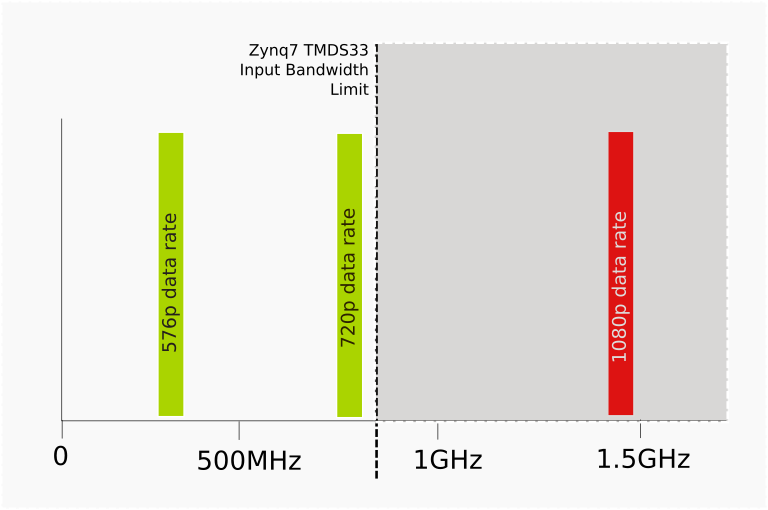
So HDMICAP is targeted at supporting 720p and below. The next generation of FPGAs coming soon are made on a smaller process and may extend the ability of TMDS33 inputs to acheive higher bandwidths, but we'll have to see.
Even though it can't reach 1080p, if something like HDMI audio works at 720p, so long as there are enough data islands at 1080p it will also work there, so being able to analyze 720p below is useful even for the resolutions that are out of range.
Capturing and deserializing the HDMI data
As I mentioned earlier back in the day a lot of tricks were neeed if you wanted FPGAs to operate at high speeds, that has improved a huge amount but there are still some design choices required to work around the fact that the programmable logic is slower than a direct implementation in silicon.
The cheap Zynq variants 7010 and 7020 don't have built-in hard SERDES (Serializer / Deserializer) blocks needed for high speed serial - parallel conversion.
That's OK, because we have an FPGA... we can roll our own deserializer. However since the data is coming at 742.5MHz, that itself is too fast for the FPGA.
To work around this, the SelectIO blocks in the FPGA support a DDR capture mode, where they capture on both edges of a clock at half the data rate. In this way we can drive it at 5x px clock rate, or 371.25MHz, and get two samples per clock. That's within the range of the FPGA logic capability, although only just, requiring extreme simplification of what's in this fast clock domain.
So the combination of the TMDS33 bandwidth limitation and DDR SelectIO support in the FPGA means we don't need the hardware SERDES - can't get any advantage from using it - and so the cheapest FPGAs found on Z-Turn are fine.
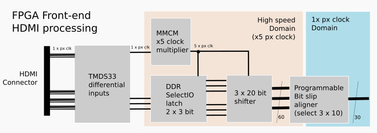
The clock and basically 3 bits of data come in at the left, go through differential -> single-ended conversion. The clock is then multiplied by 5 times and then used to sample the data on the 3-bit data bus on each edge, generating 3 x 10 samples per original pixel clock.
This is then captured into a 20-bit shifter for each channel. That's all that's in the 371.25MHz domain. The rest of the HDMI processing logic runs at the pixel clock rate of 74.25MHz which the FPGA can deal with much easier.
Because it's not known where we are in a 10-bit word in the channel bitstream, there is a per-channel programmable alignment unit that selects 10 bits from the last 20 bits. The driver uses this channel-by-channel to compare how many control symbols are captured on the channel for each of the 10 possible offsets, and picks the highest one.
At that point, we have recovered the 30 bits per pixel as a 30-bit bus coming at the pixel clock rate, which is the end of the front-end processing.
Per-channel decoders and protocol state machine
HDMI has three main codings
- 10b2b Control period coding
- 10b8b Active video coding
- 10b4b TERC4 Data Island coding
There are also a couple of extra control symbols used as part of transitioning between control period and data islands, and the active video period.
The FPGA runs all the decoders in parallel and the state machine sorts out what it must mean for what state we are in, and uses the output of the appropriate decoder accordingly.
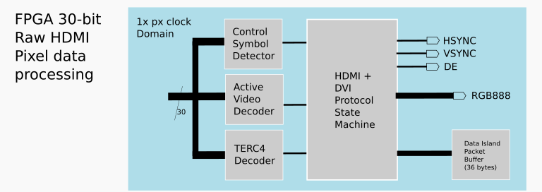
The state machine is quite complex but its main trick is that seeing a control period symbol will reset it to know it is in blanking, in this way it can reliably acquire and keep sync with the HDMI data stream.
The state machine also implements the logic to choose from where to take the hsync and vsync state during blanking, as mentioned before in HDMI that information is carried in a completely different coding when in a data island, the first channel carries it then using TERC4. The state machine produces a consistent view of the syncs hiding these details, and also DE an "Active Video Period" signal indicating the decoded pixel data is valid.
Lastly it collects together 36-byte data island packets and buffers them.
Raster measurement and statistics collection
Now reliably decoded syncs are availble, they can be measured to discover the timings of the video raster.
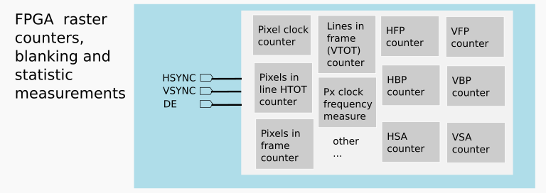
In addition, the HDMI pixel clock frequency is measured by comparing it to the known 100MHz AXI clock also available in the FPGA.
There is a specific counter for the number of pixel clocks between VSYNCs, ie, in one frame. Normally this would not be needed, since you can just multiply HTOT x VTOT to know it. However this was added because I found that is not always the case, as we will discuss later. It's an interesting case where a specific measurement was added to an FPGA-based analyzer to capture debugging information we didn't have any reason to be expect to be useful at the outset.
There are actually several other measurements done in this block such as VSYNC horizontal offset related to the above.
Interface to SoC AXI Bus
Finally an AXI peripheral is instantiated to contain the read - write registers to control everything. This appears as a normal IP on the SoC, it's set up in Device Tree and we use writel() and readl() same as we would a hardwired SoC peripheral.
A Scatter-Gather DMAC is also instantiated so the captured data can be stored on the DDR3 in realtime. There's a choice of what is DMA'd:
completely raw 30-bit captures which are unsynchronized, so you can capture data even if something is completely broken with, eg, syncs in what you are sending
raw data but frame-synchronized and the active video part converted to RGB888
capture only the data island packets (this lets you, eg, capture the raw pcm audio samples and reconstruct them into a wav file)
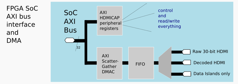
The DMAC is a full AXI DMAC with scatter-gather capabilities, it has a limitation its maximum DMA length is 8MB for one action.
In raw capture mode, you can literally hexdump the capture and see every bit that went out on the HDMI cable exactly as it was captured.
Continued
Now the FPGA hardware is described, in the the next part we take a look at the software arrangements that run on Linux on the same SoC with the FPGA.
